OneStopGate.Com
OnestopGate   OnestopGate
   Thursday, May 9, 2024 Login  
OnestopGate
Home | Overview | Syllabus | Tutorials | FAQs | Downloads | Recommended Websites | Advertise | Payments | Contact Us | Forum
OneStopGate

GATE Resources
Gate Articles
Gate Books
Gate Colleges 
Gate Downloads 
Gate Faqs
Gate Jobs
Gate News 
Gate Sample Papers
Training Institutes

GATE Overview
Overview
GATE Eligibility
Structure Of GATE
GATE Coaching Centers
Colleges Providing M.Tech/M.E.
GATE Score
GATE Results
PG with Scholarships
Article On GATE
Admission Process For M.Tech/ MCP-PhD
GATE Topper 2012-13
GATE Forum


GATE 2025 Exclusive
Organizing Institute
Important Dates
How to Apply
Discipline Codes
GATE 2025 Exam Structure

GATE 2025 Syllabus
Aerospace Engg..
Agricultural Engg..
Architecture and Planning
Chemical Engg..
Chemistry
Civil Engg..
Computer Science / IT
Electronics & Communication Engg..
Electrical Engg..
Engineering Sciences
Geology and Geophysics
Instrumentation Engineering
Life Sciences
Mathematics
Mechanical Engg..
Metallurgical Engg..
Mining Engg..
Physics
Production & Industrial Engg..
Pharmaceutical Sciences
Textile Engineering and Fibre Science

GATE Study Material
Aerospace Engg..
Agricultural Engg..
Chemical Engg..
Chemistry
Civil Engg..
Computer Science / IT
Electronics & Communication Engg..
Electrical Engg..
Engineering Sciences
Instrumentation Engg..
Life Sciences
Mathematics
Mechanical Engg..
Physics
Pharmaceutical Sciences
Textile Engineering  and Fibre Science

GATE Preparation
GATE Pattern
GATE Tips N Tricks
Compare Evaluation
Sample Papers 
Gate Downloads 
Experts View

CEED 2013
CEED Exams
Eligibility
Application Forms
Important Dates
Contact Address
Examination Centres
CEED Sample Papers

Discuss GATE
GATE Forum
Exam Cities
Contact Details
Bank Details

Miscellaneous
Advertisment
Contact Us


Home » GATE Study Material » Electrical Engineering » Basic Concepts » Electrical Circuits - Analytical Methods

Basic Concepts

Looking for GATE Preparation Material? Join & Get here now!

** Gate 2013 Question Papers.. ** CEED 2013 Results.. ** Gate 2013 Question Papers With Solutions.. ** GATE 2013 CUT-OFFs.. ** GATE 2013 Results.. **

Next>>
Electrical Circuits - Analytical Methods

Electrical Circuits - Analytical Methods Introduction

        You have learned how to use conductance matrix analysis in simple circuits.  However, the discussion in the first lesson did not give a formal algorithm for solution of these circuits.  Here are our goals for this lesson.

  • Given an electrical circuit composed of resistors, voltage sources and current sources,
    • Be able to write the conductance matrix representation for the circuit,
    • Be able to solve the conductance matrix-source voltage equation.

A General Method Of Setting Up Circuit Equations. - Writing The Node Equations

        In this section we will consider how circuit equations are generated and how different elements affect those circuit equations.  We will examine how node equations are written.

        We start by looking at a typical node - extracted from some larger circuit.  That node is shown below.

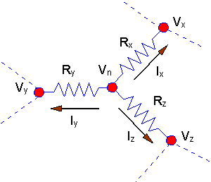
Note the following about this circuit:
  • The node shown - Node "n" - is part of a larger circuit. The resistors connected to node "n" are connected to other nodes through other resistors - shown by dotted lines in the figure.
  • We define currents flowing out of node "n" as positive when flowing away from the node. Obviously they can't all be positive, but using this convention helps in developing a formal methodology for setting up the node equations.
        The methodology that we use is as follows.
  • Define a voltage at every node in the circuit.  A typical voltage can be denoted Vn.
    • That voltage symbol,Vn, denotes the voltage at node "n" measured with respect to ground.
  • Note, that at this point we have to realize that every node voltage might not be an unknown in 
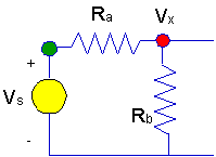
the system of equations that we are developing.  For example, in the circuit below, the voltage at the green node is known to be Vs, whereas the voltage,Vx, is not known a priori.
    • When you are setting up a group of equations to solve, it is important to know how many unknowns you have (because the level of difficulty of solution is related to the number of unknowns) and that information is important.
  • Having defined a voltage at every node, it is now possible to write KCL at nodes where the voltage   is not known.  The KCL equations have a form that we can discover from the general node above.
  • Then we write KCL at the node where Vx appears.
  • Finally, we solve whatever equation results from writing KCL.
        We will look at these two steps separately, and we will work first on the problem of writing KCL at a node.

Writing Node Equations

        Here is that node extracted from a larger circuit.

        Examining the sample node - node "n" - it is relatively easy to write the KCL equations for the node.  Using KCL for the sample node, we would have:
Ix + Iy + Iz = 0

And, each of the currents can be expressed in terms of the voltage at the node and the voltage at one of the neighboring nodes.  For example:

Ix = (Vn -Vx)/Rx

Express every current in that manner, and put those expressions into the KCL equation:

(Vn -Vx)/Rx + (Vn -Vy)/Ry + (Vn -Vz)/Rz = 0

        Notice how this equation plays out.  By defining currents as positive when they are flowing away from the node (i.e., the current arrows defining current polarity point away from the node.), every term that involves Vn turns out to have a plus sign in the resultant equation.  That gives you a way to know when you have written the equation correctly.  There is a payoff to being systematic and consistent when you write the KCL equations.  You will find almost every textbook that discusses this topic writes the equations this way!  You should adopt that practice as well, and you should never go wrong.

        The case of nodes with only resistors connected is simple enough, but there are special situations that you will need to take care of.  Here are those special cases.

  • One of the adjacent nodes might be connected to a voltage source.  Actually, there are two special cases here because the other end of the voltage source might be connected go ground - the first case -  or it might be connected to still another node - the second case.
  • There might be a current source connected to the node at which you write KCL.
        Let's consider the first case.  Here is a picture of the situation with an adjacent node connected to a grounded voltage source.

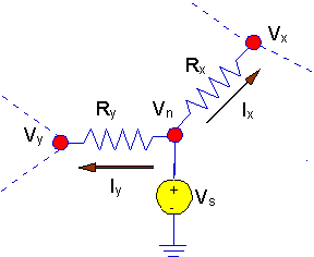
In this situation, KCL is written exactly as it was before.  However, the voltage source serves to fix a node voltage and that node voltage is no longer a variable with an unknown value.  Instead, the voltage at node 'x' in the figure is known to be Vs.  After you have written KCL at the node, when you go to solve the KCL equations simultaneously, that known value will appear in a term on the right hand side (the knowns) of the equation.  Thus:

  • If there is a grounded source connected to node "n", then:
    • No KCL equation is written at node "n".
    • We have Vn = Vs.
        There is another case in which there is a voltage source connected between two nodes - neither of which is ground.  In this case the voltage source establishes a voltage difference between two nodes, and the way this situation is handled is slightly different.
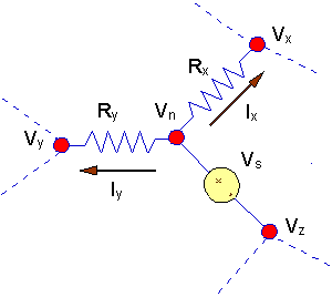
  • If there is an ungrounded source connected between node "n" and node "z", then
    • Vn = Vz + Vs.
  • If Vz can be found, thenVz is known from this equation.
  • One less KCL equation will be written for this circuit.
  • Then, the approach would be to write a KCL equation at either node "n" or node "z", and use the equationVn = Vz + Vs to find the voltage at the other node.
  • The implication is that one less KCL equation will be written.
Next>>


Discussion Center

Discuss/
Query

Papers/
Syllabus

Feedback/
Suggestion

Yahoo
Groups

Sirfdosti
Groups

Contact
Us

MEMBERS LOGIN
  
Email ID:
Password:

  Forgot Password?
 New User? Register!

INTERVIEW EBOOK
Get 9,000+ Interview Questions & Answers in an eBook. Interview Question & Answer Guide
  • 9,000+ Interview Questions
  • All Questions Answered
  • 5 FREE Bonuses
  • Free Upgrades
GATE RESOURCES
 
  • Gate Books
  • Training Institutes
  • Gate FAQs
  • GATE BOOKS
     
  • Mechanical Engineeering Books
  • Robotics Automations Engineering Books
  • Civil Engineering Books
  • Chemical Engineering Books
  • Environmental Engineering Books
  • Electrical Engineering Books
  • Electronics Engineering Books
  • Information Technology Books
  • Software Engineering Books
  • GATE Preparation Books
  • Exciting Offers


    GATE Exam, Gate 2009, Gate Papers, Gate Preparation & Related Pages


    GATE Overview | GATE Eligibility | Structure Of GATE | GATE Training Institutes | Colleges Providing M.Tech/M.E. | GATE Score | GATE Results | PG with Scholarships | Article On GATE | GATE Forum | GATE 2009 Exclusive | GATE 2009 Syllabus | GATE Organizing Institute | Important Dates for GATE Exam | How to Apply for GATE | Discipline / Branch Codes | GATE Syllabus for Aerospace Engineering | GATE Syllabus for Agricultural Engineering | GATE Syllabus for Architecture and Planning | GATE Syllabus for Chemical Engineering | GATE Syllabus for Chemistry | GATE Syllabus for Civil Engineering | GATE Syllabus for Computer Science / IT | GATE Syllabus for Electronics and Communication Engineering | GATE Syllabus for Engineering Sciences | GATE Syllabus for Geology and Geophysics | GATE Syllabus for Instrumentation Engineering | GATE Syllabus for Life Sciences | GATE Syllabus for Mathematics | GATE Syllabus for Mechanical Engineering | GATE Syllabus for Metallurgical Engineering | GATE Syllabus for Mining Engineering | GATE Syllabus for Physics | GATE Syllabus for Production and Industrial Engineering | GATE Syllabus for Pharmaceutical Sciences | GATE Syllabus for Textile Engineering and Fibre Science | GATE Preparation | GATE Pattern | GATE Tips & Tricks | GATE Compare Evaluation | GATE Sample Papers | GATE Downloads | Experts View on GATE | CEED 2009 | CEED 2009 Exam | Eligibility for CEED Exam | Application forms of CEED Exam | Important Dates of CEED Exam | Contact Address for CEED Exam | CEED Examination Centres | CEED Sample Papers | Discuss GATE | GATE Forum of OneStopGATE.com | GATE Exam Cities | Contact Details for GATE | Bank Details for GATE | GATE Miscellaneous Info | GATE FAQs | Advertisement on GATE | Contact Us on OneStopGATE |
    Copyright © 2024. One Stop Gate.com. All rights reserved Testimonials |Link To Us |Sitemap |Privacy Policy | Terms and Conditions|About Us
    Our Portals : Academic Tutorials | Best eBooksworld | Beyond Stats | City Details | Interview Questions | India Job Forum | Excellent Mobiles | Free Bangalore | Give Me The Code | Gog Logo | Free Classifieds | Jobs Assist | Interview Questions | One Stop FAQs | One Stop GATE | One Stop GRE | One Stop IAS | One Stop MBA | One Stop SAP | One Stop Testing | Web Hosting | Quick Site Kit | Sirf Dosti | Source Codes World | Tasty Food | Tech Archive | Software Testing Interview Questions | Free Online Exams | The Galz | Top Masala | Vyom | Vyom eBooks | Vyom International | Vyom Links | Vyoms | Vyom World
    C Interview Questions | C++ Interview Questions | Send Free SMS | Placement Papers | SMS Jokes | Cool Forwards | Romantic Shayari