OneStopGate.Com
OnestopGate   OnestopGate
   Saturday, December 21, 2024 Login  
OnestopGate
Home | Overview | Syllabus | Tutorials | FAQs | Downloads | Recommended Websites | Advertise | Payments | Contact Us | Forum
OneStopGate

GATE Resources
Gate Articles
Gate Books
Gate Colleges 
Gate Downloads 
Gate Faqs
Gate Jobs
Gate News 
Gate Sample Papers
Training Institutes

GATE Overview
Overview
GATE Eligibility
Structure Of GATE
GATE Coaching Centers
Colleges Providing M.Tech/M.E.
GATE Score
GATE Results
PG with Scholarships
Article On GATE
Admission Process For M.Tech/ MCP-PhD
GATE Topper 2012-13
GATE Forum


GATE 2025 Exclusive
Organizing Institute
Important Dates
How to Apply
Discipline Codes
GATE 2025 Exam Structure

GATE 2025 Syllabus
Aerospace Engg..
Agricultural Engg..
Architecture and Planning
Chemical Engg..
Chemistry
Civil Engg..
Computer Science / IT
Electronics & Communication Engg..
Electrical Engg..
Engineering Sciences
Geology and Geophysics
Instrumentation Engineering
Life Sciences
Mathematics
Mechanical Engg..
Metallurgical Engg..
Mining Engg..
Physics
Production & Industrial Engg..
Pharmaceutical Sciences
Textile Engineering and Fibre Science

GATE Study Material
Aerospace Engg..
Agricultural Engg..
Chemical Engg..
Chemistry
Civil Engg..
Computer Science / IT
Electronics & Communication Engg..
Electrical Engg..
Engineering Sciences
Instrumentation Engg..
Life Sciences
Mathematics
Mechanical Engg..
Physics
Pharmaceutical Sciences
Textile Engineering  and Fibre Science

GATE Preparation
GATE Pattern
GATE Tips N Tricks
Compare Evaluation
Sample Papers 
Gate Downloads 
Experts View

CEED 2013
CEED Exams
Eligibility
Application Forms
Important Dates
Contact Address
Examination Centres
CEED Sample Papers

Discuss GATE
GATE Forum
Exam Cities
Contact Details
Bank Details

Miscellaneous
Advertisment
Contact Us


Home » GATE Study Material » Electronics and Telecommunication » Electronic Circuits and Design » PIN diode attenuator

PIN diode attenuator

Looking for GATE Preparation Material? Join & Get here now!

** Gate 2013 Question Papers.. ** CEED 2013 Results.. ** Gate 2013 Question Papers With Solutions.. ** GATE 2013 CUT-OFFs.. ** GATE 2013 Results.. **

PIN diode attenuator

PIN diode attenuator


- a constant impedance attenuator design for radio frequency or RF circuit design applications


Electronically controllable PIN diode attenuators are often used in radio frequency or RF circuit designs. It is often necessary to be able to control the level of a radio frequency signal using a control voltage. It is possible to achieve this using a PIN diode attenuator circuit. Some circuits do not offer a constant impedance, whereas this PIN diode attenuator gives a satisfactory match.

The PIN diode variable attenuator is used to give attenuation over a range of about 20 dB and can be used in 50 ohm systems. The inductor L1 along with the capacitors C4 and C5 are included to prevent signal leakage from D1 to D2 that would impair the performance of the circuit.

The maximum attenuation is achieved when Vin is at a minimum. At this point current from the supply V+ turns the diodes D1 and D2 on effectively shorting the signal to ground. D3 is then reverse biased. When Vin is increased the diodes D1 and D2 become reverse biased, and D3 becomes forward biased, allowing the signal to pass through the circuit.
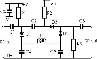
PIN diode variable attenuator

PIN diode variable attenuator


Typical values for the circuit might be: +V : 5 volts; Vin : 0 - 6 volts; D1 to D3 HP5082-3080 PIN diodes; R1 2k2; R2 : 1k; R3 2k7; L1 is self resonant above the operating frequency, but sufficient to give isolation between the diodes D1 and D2.

These values are only a starting point for an experimental design, and are only provided as such. The circuit may not be suitable in all instances.


Choice of diode


Although in theory any diode could be used in this position, PIN diodes have a number of advantages as switches. In the first place they are more linear than ordinary PN junction diodes. This means that in their action as a radio frequency switch they do not create as many spurious products and additionally as an attenuator they have a more useful curve. Secondly when reverse biased and switched off, the depletion layer is wider than with an ordinary diode and this provides for greater isolation when switching.


Discussion Center

Discuss/
Query

Papers/
Syllabus

Feedback/
Suggestion

Yahoo
Groups

Sirfdosti
Groups

Contact
Us

MEMBERS LOGIN
  
Email ID:
Password:

  Forgot Password?
 New User? Register!

INTERVIEW EBOOK
Get 9,000+ Interview Questions & Answers in an eBook. Interview Question & Answer Guide
  • 9,000+ Interview Questions
  • All Questions Answered
  • 5 FREE Bonuses
  • Free Upgrades
GATE RESOURCES
 
  • Gate Books
  • Training Institutes
  • Gate FAQs
  • GATE BOOKS
     
  • Mechanical Engineeering Books
  • Robotics Automations Engineering Books
  • Civil Engineering Books
  • Chemical Engineering Books
  • Environmental Engineering Books
  • Electrical Engineering Books
  • Electronics Engineering Books
  • Information Technology Books
  • Software Engineering Books
  • GATE Preparation Books
  • Exciting Offers


    GATE Exam, Gate 2009, Gate Papers, Gate Preparation & Related Pages


    GATE Overview | GATE Eligibility | Structure Of GATE | GATE Training Institutes | Colleges Providing M.Tech/M.E. | GATE Score | GATE Results | PG with Scholarships | Article On GATE | GATE Forum | GATE 2009 Exclusive | GATE 2009 Syllabus | GATE Organizing Institute | Important Dates for GATE Exam | How to Apply for GATE | Discipline / Branch Codes | GATE Syllabus for Aerospace Engineering | GATE Syllabus for Agricultural Engineering | GATE Syllabus for Architecture and Planning | GATE Syllabus for Chemical Engineering | GATE Syllabus for Chemistry | GATE Syllabus for Civil Engineering | GATE Syllabus for Computer Science / IT | GATE Syllabus for Electronics and Communication Engineering | GATE Syllabus for Engineering Sciences | GATE Syllabus for Geology and Geophysics | GATE Syllabus for Instrumentation Engineering | GATE Syllabus for Life Sciences | GATE Syllabus for Mathematics | GATE Syllabus for Mechanical Engineering | GATE Syllabus for Metallurgical Engineering | GATE Syllabus for Mining Engineering | GATE Syllabus for Physics | GATE Syllabus for Production and Industrial Engineering | GATE Syllabus for Pharmaceutical Sciences | GATE Syllabus for Textile Engineering and Fibre Science | GATE Preparation | GATE Pattern | GATE Tips & Tricks | GATE Compare Evaluation | GATE Sample Papers | GATE Downloads | Experts View on GATE | CEED 2009 | CEED 2009 Exam | Eligibility for CEED Exam | Application forms of CEED Exam | Important Dates of CEED Exam | Contact Address for CEED Exam | CEED Examination Centres | CEED Sample Papers | Discuss GATE | GATE Forum of OneStopGATE.com | GATE Exam Cities | Contact Details for GATE | Bank Details for GATE | GATE Miscellaneous Info | GATE FAQs | Advertisement on GATE | Contact Us on OneStopGATE |
    Copyright © 2024. One Stop Gate.com. All rights reserved Testimonials |Link To Us |Sitemap |Privacy Policy | Terms and Conditions|About Us
    Our Portals : Academic Tutorials | Best eBooksworld | Beyond Stats | City Details | Interview Questions | India Job Forum | Excellent Mobiles | Free Bangalore | Give Me The Code | Gog Logo | Free Classifieds | Jobs Assist | Interview Questions | One Stop FAQs | One Stop GATE | One Stop GRE | One Stop IAS | One Stop MBA | One Stop SAP | One Stop Testing | Web Hosting | Quick Site Kit | Sirf Dosti | Source Codes World | Tasty Food | Tech Archive | Software Testing Interview Questions | Free Online Exams | The Galz | Top Masala | Vyom | Vyom eBooks | Vyom International | Vyom Links | Vyoms | Vyom World
    C Interview Questions | C++ Interview Questions | Send Free SMS | Placement Papers | SMS Jokes | Cool Forwards | Romantic Shayari