ElectroStatic Discharge (ESD) tutorial [2]
a tutorial or summary about the basics of Electro Static Discharge, ESD
and the affects it has on electronic components and electronic circuits
ESD can have disastrous effects on electronic components.
With ICs operating of supply voltages of 5 V and less these days, and with the
feature sizes measured in fractions of a micron the static charges that go
unnoticed in everyday life can easily destroy a chip. Worse still these effects
may not destroy the chip instantly, but leave a defect waiting to cause a
problem later in the life of the equipment.
In view of their sensitivity to static, most semiconductor
devices today are treated as static sensitive devices ( SSD ). To prevent damage
they must be handled in anti-static areas, often called ESDPAs (Electrostatic
Protected Areas). Within these areas a variety of precautions are taken to
ensure that static is dissipated and that the SSD, static sensitive devices do
not experience any static discharges. Benches with dissipative surfaces,
anti-static flooring, wrist straps for oerpators and many more items all form
part of these anti-static areas.
Sensitivity
Some electronic devices are more sensitive to ESD than
others. However to put the problem in perspective it is worth relating the
levels of static to those to supply voltages. One would not consider applying a
voltage of even fifty volts to a logic device. Yet static voltages of several
kilovolts are often applied to them by careless handling.
The devices that are most sensitive to ESD are generally
those which include FETs. These devices have very high impedances which do not
allow the charge to dissipate in a more controlled fashion. However this does
not mean that bipolar devices are immune from damage.
Standard CMOS chips can be damaged by static voltages of as
little as 250V. These include the 74HC and 74HCT logic families are widely used
in many designs using "glue logic" because of their lower current consumption.
However many of the new microprocessors and LSI chips use very much smaller
feature sizes, and cannot withstand anything like these voltages, making them
very sensitive to ESD. Many new devices would be destroyed by operating them
with a supply voltage of 5 V, and they are corresponding more susceptible to
damage from ESD.
Logic devices are not the only devices requiring anti static
precautions to be taken. GaAsFETs which are used for RF applications are very
susceptible to damage, and can be destroyed by static voltages as low as 100V.
Other forms of discrete FETs are also affected by ESD. MOSFETs which are again
often used for many RF applications are very sensitive.
Even ordinary bipolar transistors can be damaged by
potentials of around 500V. This is particularly true of the newer transistors
which are likely to have much smaller internal geometries to give higher
operating frequencies. This is only a broad indication of a very few of the ESD
susceptibility levels. However it indicates that all semiconductor devices
should be treated as static sensitive devices ( SSD ).
It is not only semiconductor devices that are being treated
as SSDs these days. In some areas even passive components are starting to be
treated as static sensitive. With the ever quickening trend to miniaturisation
individual components are becoming much smaller. This makes them more sensitive
to the effects of damage from ESD. A large discharge through a very small
component may cause overheating, or breakdown in the component.
Discharge mechanisms
The way in which the electrostatic discharge, ESD, takes
place is dependent on a large number of variables. Most of these are difficult
to quantify. The level of static which is built up varies according to the
materials involved, the humidity of the day, and even the size of the person has
an effect. Each person represents a capacitor on which charge is held. The
average person represents a capacitor of about 300 pF but this will vary greatly
from one person to the next.
The way in which the discharge takes place also varies. Often
the charge will be dissipated very quickly: typically in less than a hundred
nanoseconds. During this time the peak current can rise to as much as twenty or
thirty amps. The peak current and the time for the discharge are dependent upon
a wide variety of factors. However if a metal object is used, like a pair of
tweezers or thin nosed pliers the current peak is higher and reached in a
shorter time than if the discharge takes place through a finger. This is because
the metal provides a much lower resistance path for the discharge. However
whatever the means of the discharge, the same amount of charge will be
dissipated.
Failure mechanisms
The way in which ICs fail as a result of ESD also varies, and
it is also dependent upon a number of factors including the way in which the
charge is dissipated to the topology within the IC.
One of the most obvious way in which an IC can fail as a
result of ESD occurs when the static charge represented as a very high voltage
gives rise to a high peak current causing burn out. Even though the current
passes for a very short time, the minute sizes within ICs can mean that the
small interconnecting links wires or the devices in the chip itself can be fused
by the amount of heat dissipated. In some instances the connection or component
may not be completely destroyed. Instead it may only be partly destroyed. When
this happens the device will continue to operate and may have no detectable
reduction in its performance. At other times there may be a slight degradation
in operation. This is particularly true of analogue devices where small
fragments of material from the area of damage can spread over the surface of the
chip. These may bridge or particularly bridge other components in the chip
causing the performance to be altered or degraded.
When damage has been caused to the device, but it still
remains operational, the defect leaves it with what is termed a 'latent defect'
which may lead to a failure later in its life. Subsequent current surges
resulting from turning the equipment on, or even as a result of normal operation
may stress the defect and cause it to fail. This may also be brought about by
vibration in some cases.
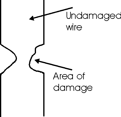
Latent damage cause inside an IC by ESD
These latent defects are particularly damaging because they
are likely to lead to failures later in the life of the equipment, thereby
reducing its reliability. In fact manufacturing plants with poor anti-static
protection are likely to produce low reliability equipment as a result of this.
In fact it is estimated that for every device which suffers instant damage at
least ten are affected by latent damage and will fail at a later date.
Another way in which ESD can cause failure is when the
voltage itself causes breakdown within the IC. It is quite possible for the
voltage to breakdown an insulating oxide layer leaving the IC permanently
damaged. Again this can destroy the chip immediately, or leave a partly damaged
area with a latent failure.
Charge can also be transferred to electronic components in
other ways and cause damage. It may result in damage either from voltage
breakdown or by generating current to flow in the device. This may occur because
a highly charged item will tend to induce an opposite charge in any article near
it. Plastic drinks cups are very susceptible to carrying high static voltages
and if they are placed on a work surface next to a sensitive piece of
electronics they can induce a charge which may lead to damage.
Investigations
Although it is not easy to determine the cause of destruction
of a device, some specialist laboratories have the means of making these
investigations. They accomplish this by removing the top of the IC to reveal the
silicon chip beneath. This is inspected using a microscope to reveal the area of
damage.
These investigations are relatively costly. They are not
normally undertaken for routine failures. Instead they are only undertaken when
it is necessary to determine the exact cause of the failure.
Protection
With ICs being prone to damage so easily, it is necessary to
consider all semiconductor devices, and often many passive devices as static
sensitive devices SSD. They should only be handled in the special anti static
ESDPAs. The next page in this tutorial ( Page [3] )summarises some of the
methods and techniques that can be used. These include measures such as the use
of ESD workbenches or ESD mats, ESD wrist straps, ESD bags and ESD packaging,
etc..
|


